Ultimate Guide to Silicon Wafer Cutting: Challenges & Diamond Wire Solutions
The demand for high-quality semiconductors and solar panels is skyrocketing. Consequently, mastering efficient silicon wafer cutting is more critical than ever. When you process monocrystalline silicon, you face a hard, brittle material that shatters easily. Therefore, achieving low-loss, precise cuts is the ultimate challenge for your production line. Today, advanced multi-wire diamond sawing offers the best approach. As a leading manufacturer with over 20 years of innovation, Z-LION provides the technical insights you need. This guide breaks down the core methods and introduces our advanced electroplated diamond wire solutions to boost your efficiency.
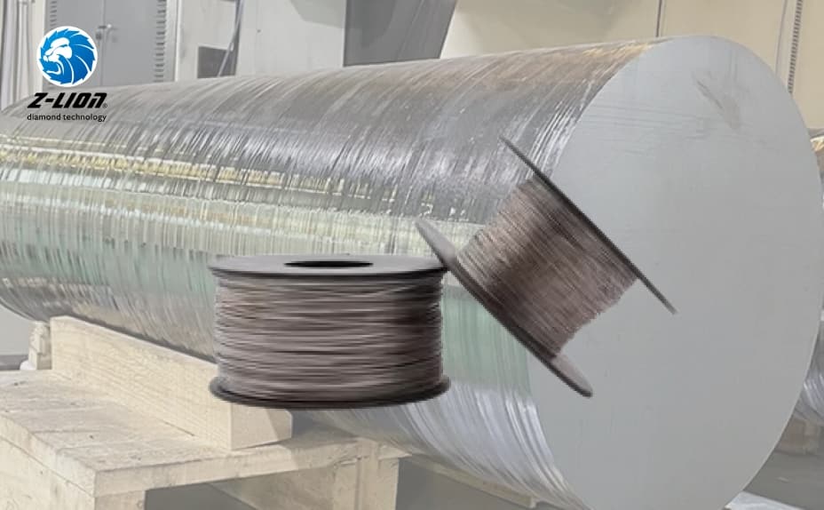
Demystifying Silicon Wafer Cutting: Slicing vs. Dicing
Before upgrading your tools, you must understand the two primary stages of silicon wafer cutting. These stages require entirely different equipment and consumables.
Feature Wafer Slicing Wafer Dicing Input Material Raw silicon ingot (boule) Processed, finished wafer Output Blank, thin silicon wafers Individual microchips (dies) Primary Tool Multi-wire diamond saws Mechanical blades or lasers Core Goal Minimize kerf loss and TTV Prevent micro-cracks on circuits
Why is silicon hard to cut? Monocrystalline silicon possesses extreme hardness and brittleness. Therefore, you need cutting tools that remain exceptionally sharp while resisting rapid wear.
The Dominance of Multi-Wire Diamond Sawing (MWDS) in Wafer Slicing
For decades, manufacturers used loose-abrasive slurry sawing. Today, Multi-Wire Diamond Sawing (MWDS) completely dominates the silicon wafer cutting industry. MWDS utilizes a web of hundreds of ultra-thin wires that carry fixed diamond particles. As a result, the machine slices through the entire silicon ingot simultaneously.
Why should you use MWDS?
Faster Cutting Speeds: Diamond wire cuts aggressively, reducing cycle times.
Thinner Wafers: You can achieve much thinner slices without breaking the material.
Better Surface Quality: The fixed abrasives leave fewer deep scratches on the silicon surface.
The wire itself acts as the most critical factor. A thinner wire directly translates to higher manufacturing yields.
Top 3 Challenges in Silicon Slicing
Even with modern equipment, you will encounter significant hurdles during silicon wafer cutting. Here are the top three challenges and a quick checklist to diagnose them.
Challenge 1: Kerf Loss. Silicon material is incredibly expensive. The width of your cut (kerf) turns valuable silicon into useless dust. Minimizing this loss is essential for profitability.
Challenge 2: Surface Defects. Poor cutting mechanics cause Total Thickness Variation (TTV), bow, warp, and micro-cracks. Consequently, these defects lead to wafer rejection during polishing.
Challenge 3: Tool Wear and Downtime. Snapped wires halt your entire production line. Therefore, durable wire is non-negotiable.
Diagnostic Checklist for Silicon Slicing:
Experiencing high TTV? Check your wire tension and ensure the diamond grit uniformity of your wire.
Losing too much raw material? Measure your current kerf loss and switch to a thinner wire diameter.
Facing frequent wire breaks? Evaluate your cutting speed and the tensile strength of your current wire.
The Solution: Z-LION Electroplated Diamond Wire
To overcome these production hurdles, you need specialized consumables. The Z-LION ZL-EW Electroplated Diamond Wire is engineered specifically for super-hard, brittle materials like silicon, ceramic, and glass.
How does this wire optimize your silicon wafer cutting process?
High Sharpness and Precision: Our advanced electroplating technology secures the diamond grit firmly. This design guarantees clean cuts. You directly reduce TTV and prevent micro-cracks.
Reduced Kerf Loss: We manufacture ultra-thin wire diameters. As a result, you waste less silicon material and generate more wafers per ingot.
Exceptional Durability: The robust electroplated bond extends the wire's lifespan. You will experience fewer wire breaks. This reliability drastically reduces your expensive machine downtime.
Partnering with Z-LION for Your Production Needs
Choosing the right supplier matters just as much as choosing the right wire. Z-LION is a publicly listed enterprise holding 63 patents. We leverage over two decades of R&D expertise. Our motto is simple: "Leadership begins with innovation."
Furthermore, we align with the "Green Z-LION" initiative. We actively develop high-efficiency, low-exhaust, and low-consumption tools. This commitment helps you meet strict ESG standards within the global semiconductor supply chain.
Are you ready to optimize your silicon processing lines? Reduce your kerf loss and increase your wafer yield today. Please contact our technical sales team to request a customized quote for your manufacturing facility.
FAQs
What is swarf and how is it managed?
The cutting process generates fine silicon dust known as swarf. Mixing this dust with cutting fluids forms a slurry waste. Modern facilities utilize advanced filtration systems to separate the silicon powder from the coolant. This separation allows operators to recycle the fluid and reduce environmental impact.
How does diamond wire wear affect production costs?
Worn wire cuts slower and creates a wider kerf. This widens the cut and increases silicon waste. Additionally, a dull wire requires higher cutting forces. High force causes wafer micro-cracks. Replacing low-quality wire frequently leads to costly machine downtime and lost revenue.
-
Online service
-
Official wechat account

-
QQ:844389055
-
E-mail:VIP@zliontools.com
Online Message
Please feel free to give your inquiry in the form below. We will reply you in 24 hours.